PCB Factory
Explorations Dan Chen / August 30, 2015
https://youtu.be/iFZ9p5ygXMI
![DSC05826](https://i0.wp.com/dankc.com/wp-content/uploads/2016/08/DSC05826.jpg?resize=628%2C419&ssl=1)
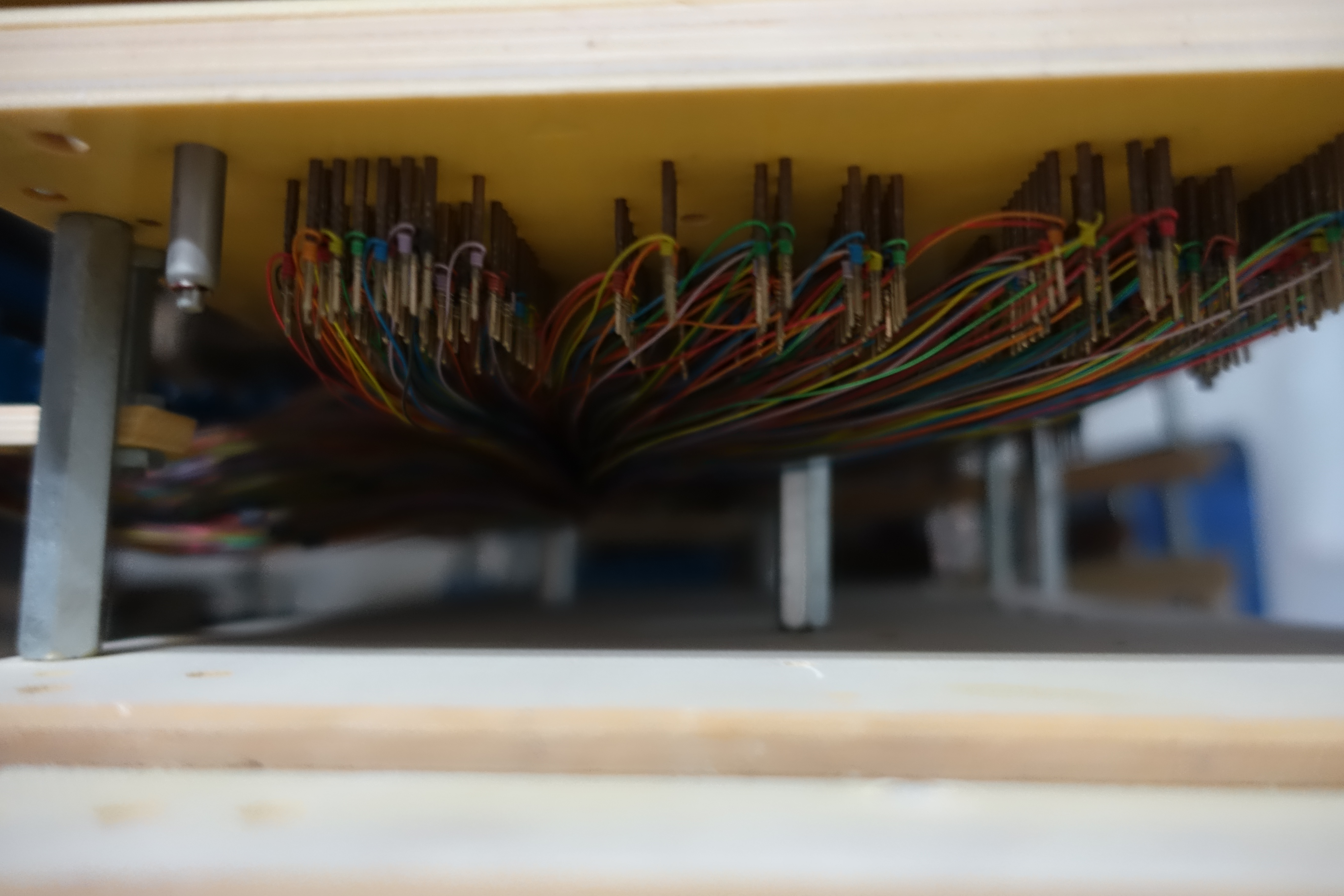
Test Jig, good for large quantity of PCBs. It’s fast but expensive, that is why large quantity could off set the cost.
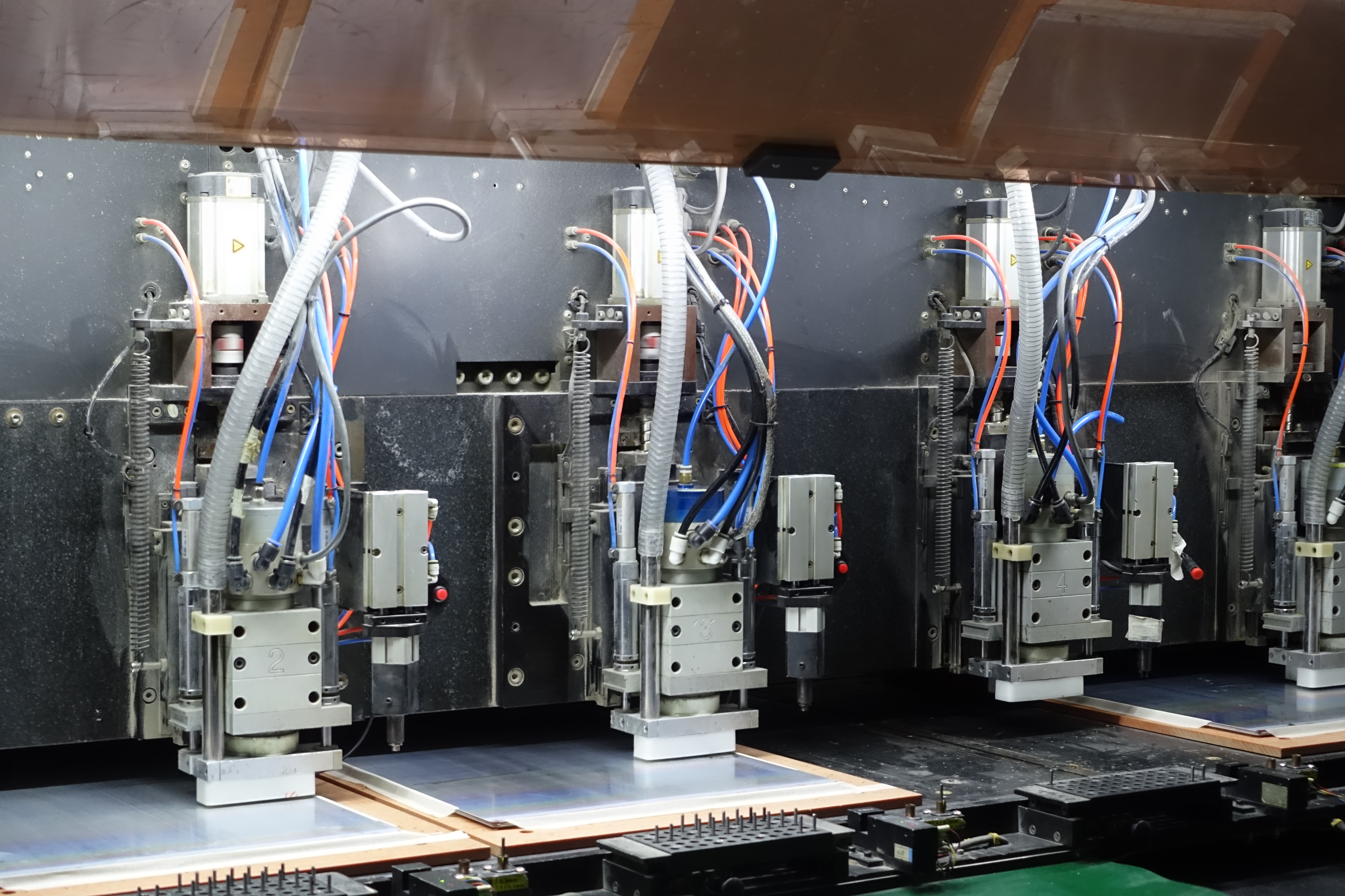
![DSC05829](https://i0.wp.com/dankc.com/wp-content/uploads/2016/08/DSC05829.jpg?resize=628%2C419&ssl=1)
Through hole drill.
![DSC05847](https://i0.wp.com/dankc.com/wp-content/uploads/2016/08/DSC05847.jpg?resize=628%2C419&ssl=1)
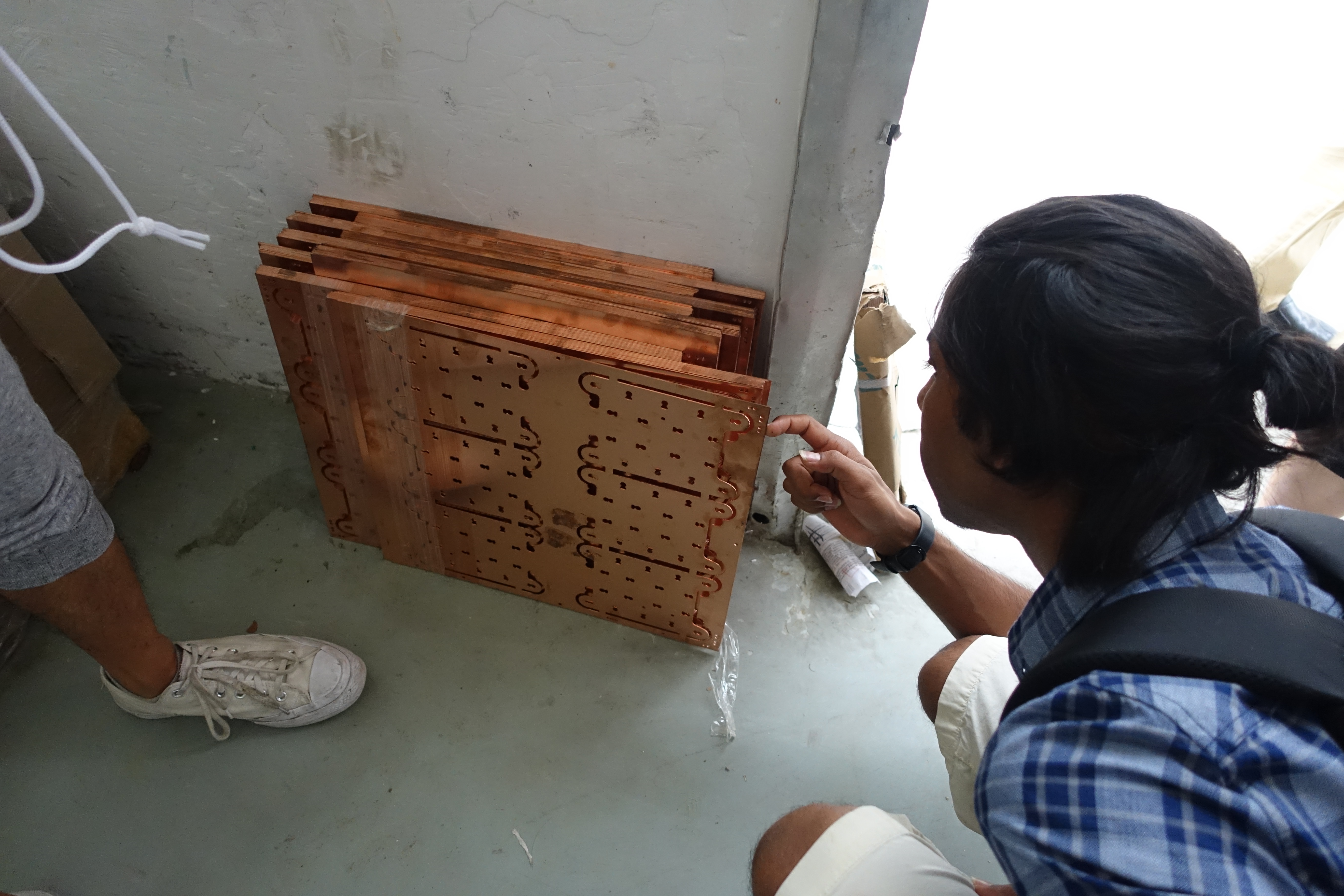
Thick PCB copper layer for high current application.
![DSC05853](https://i0.wp.com/dankc.com/wp-content/uploads/2016/08/DSC05853.jpg?resize=628%2C419&ssl=1)
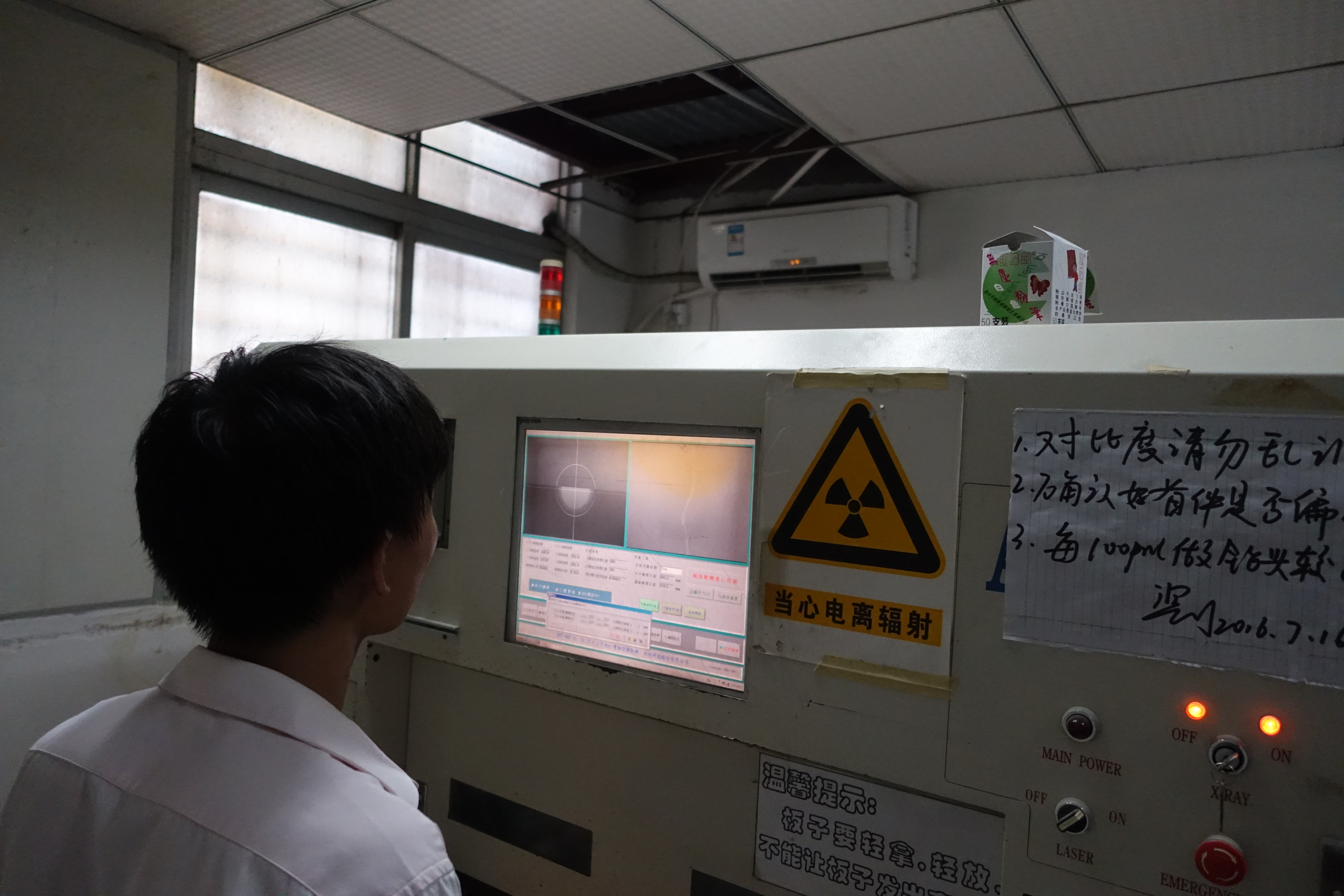
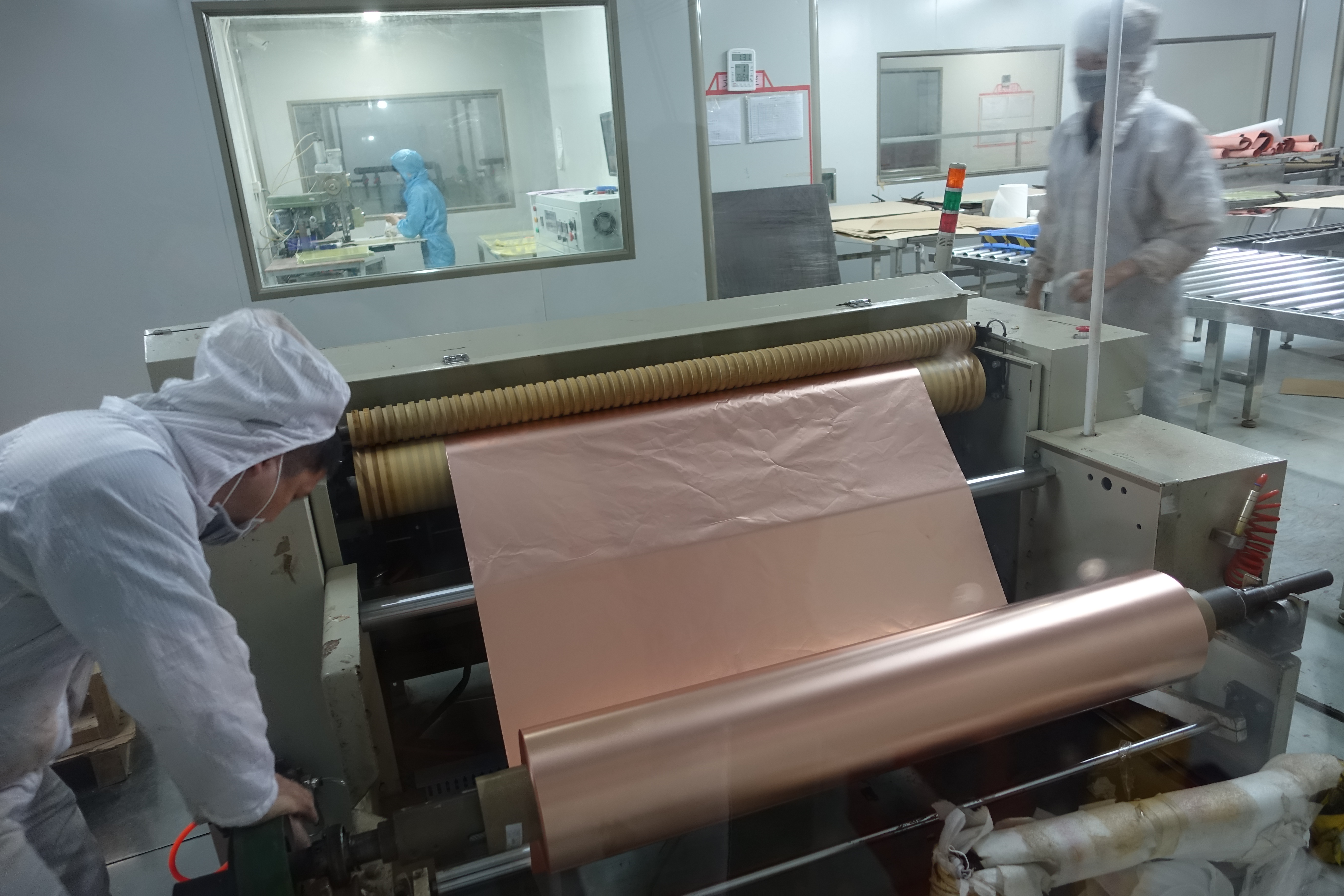
Using X-Ray to locate copper sheet covered PCB
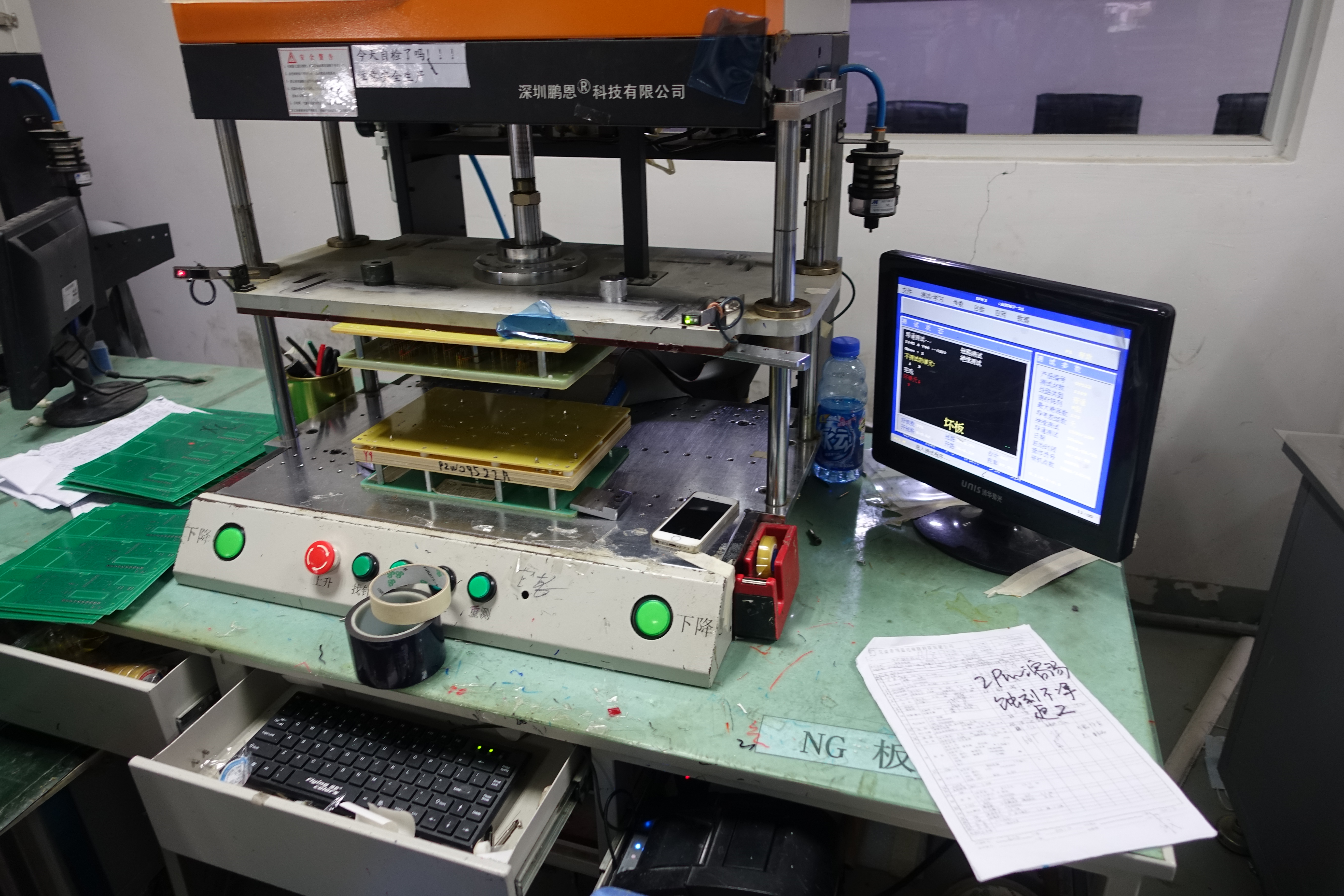
![DSC05864](https://i0.wp.com/dankc.com/wp-content/uploads/2016/08/DSC05864.jpg?resize=628%2C419&ssl=1)
Test Jig
![DSC05870](https://i0.wp.com/dankc.com/wp-content/uploads/2016/08/DSC05870.jpg?resize=628%2C419&ssl=1)
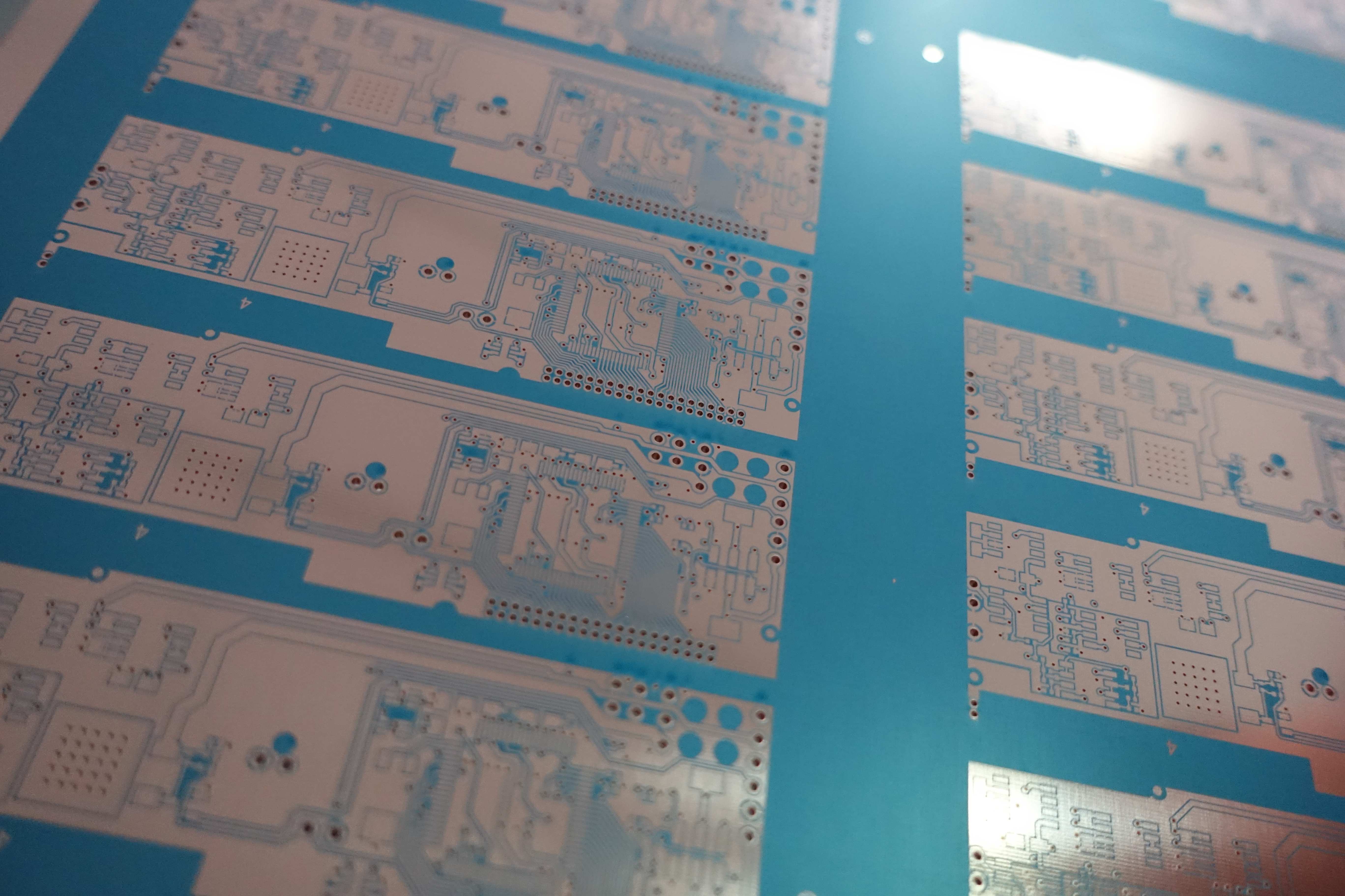
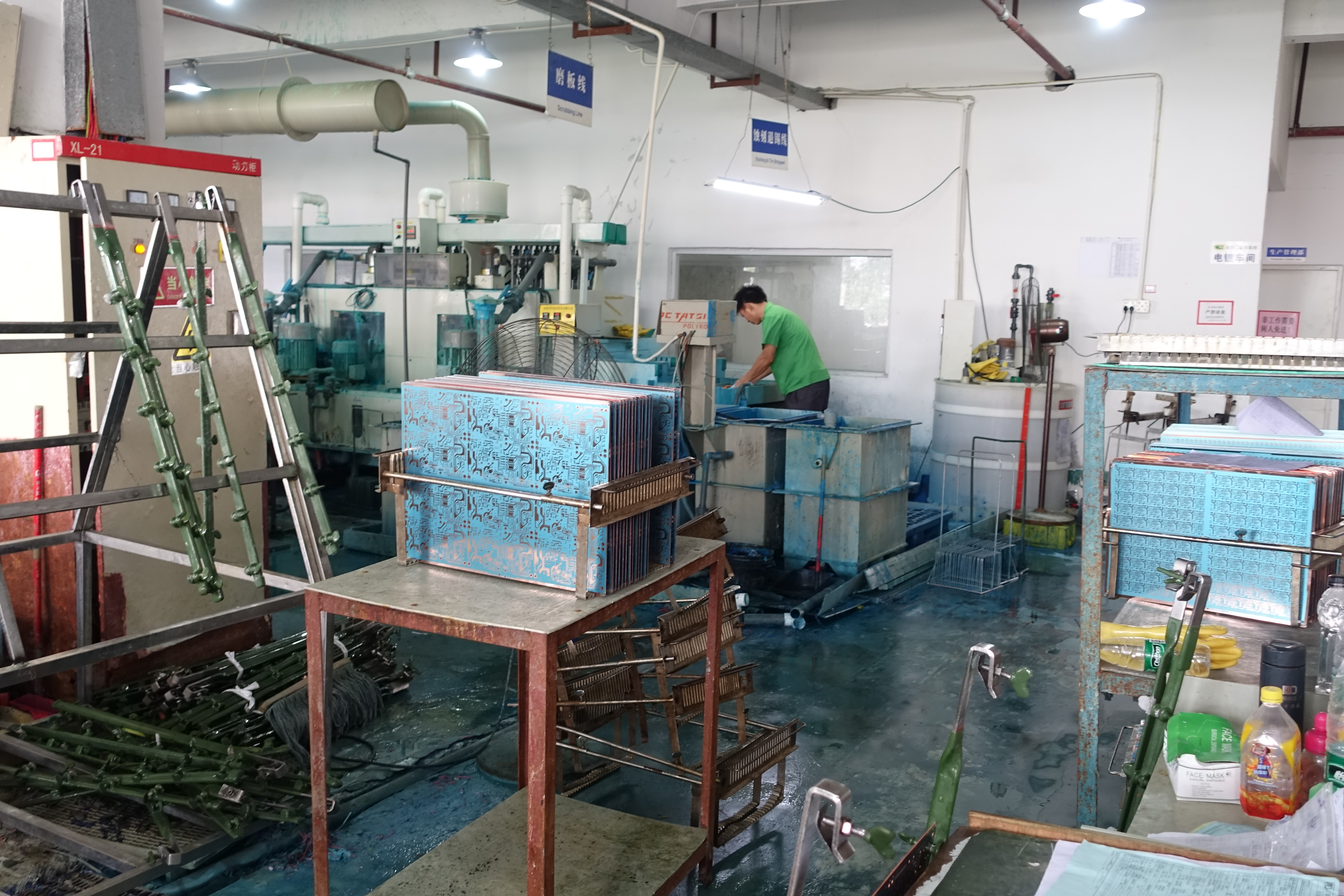
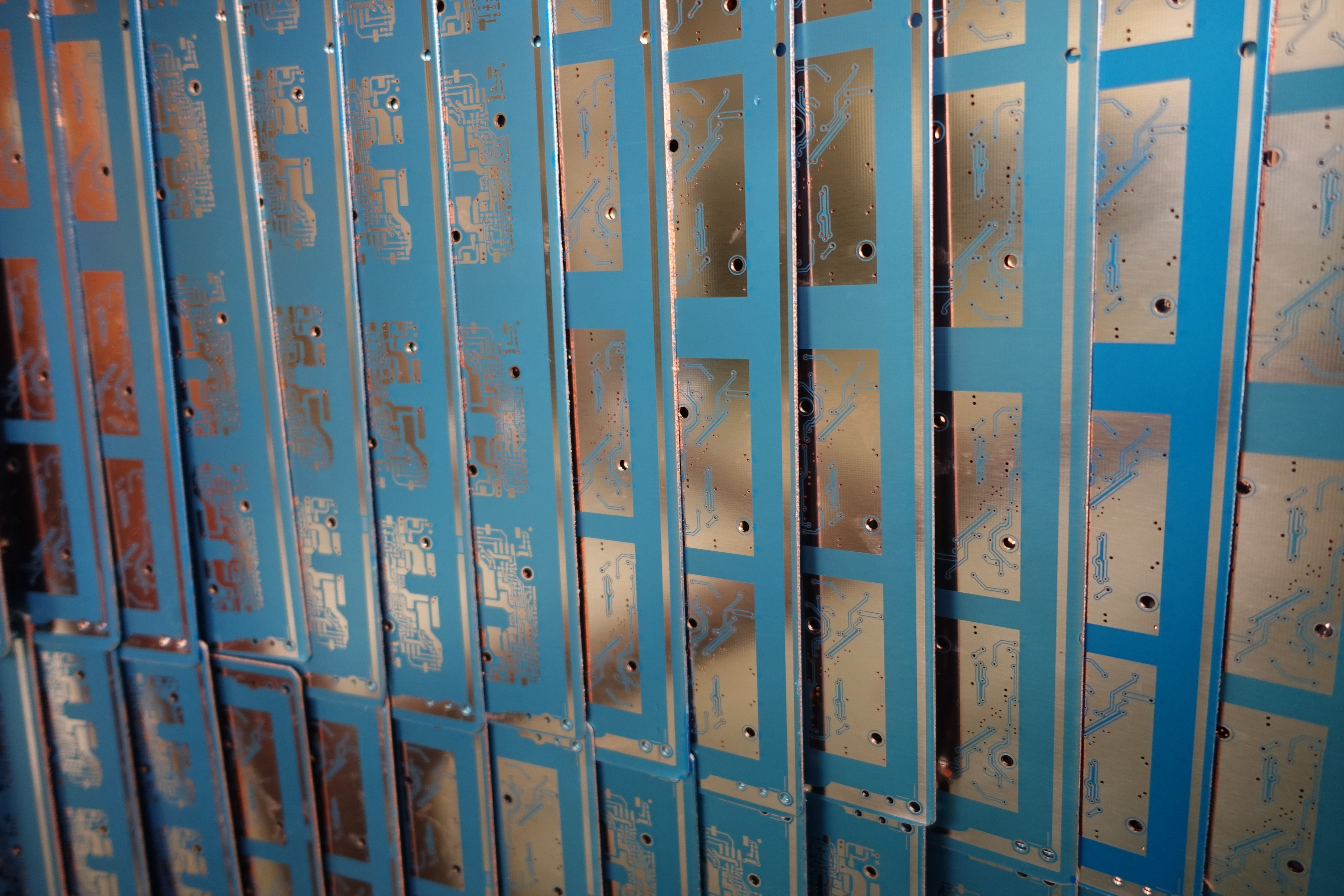
Etched PCB ready for electroplating.
![DSC05877](https://i0.wp.com/dankc.com/wp-content/uploads/2016/08/DSC05877.jpg?resize=628%2C419&ssl=1)
This factory makes large size PCBs
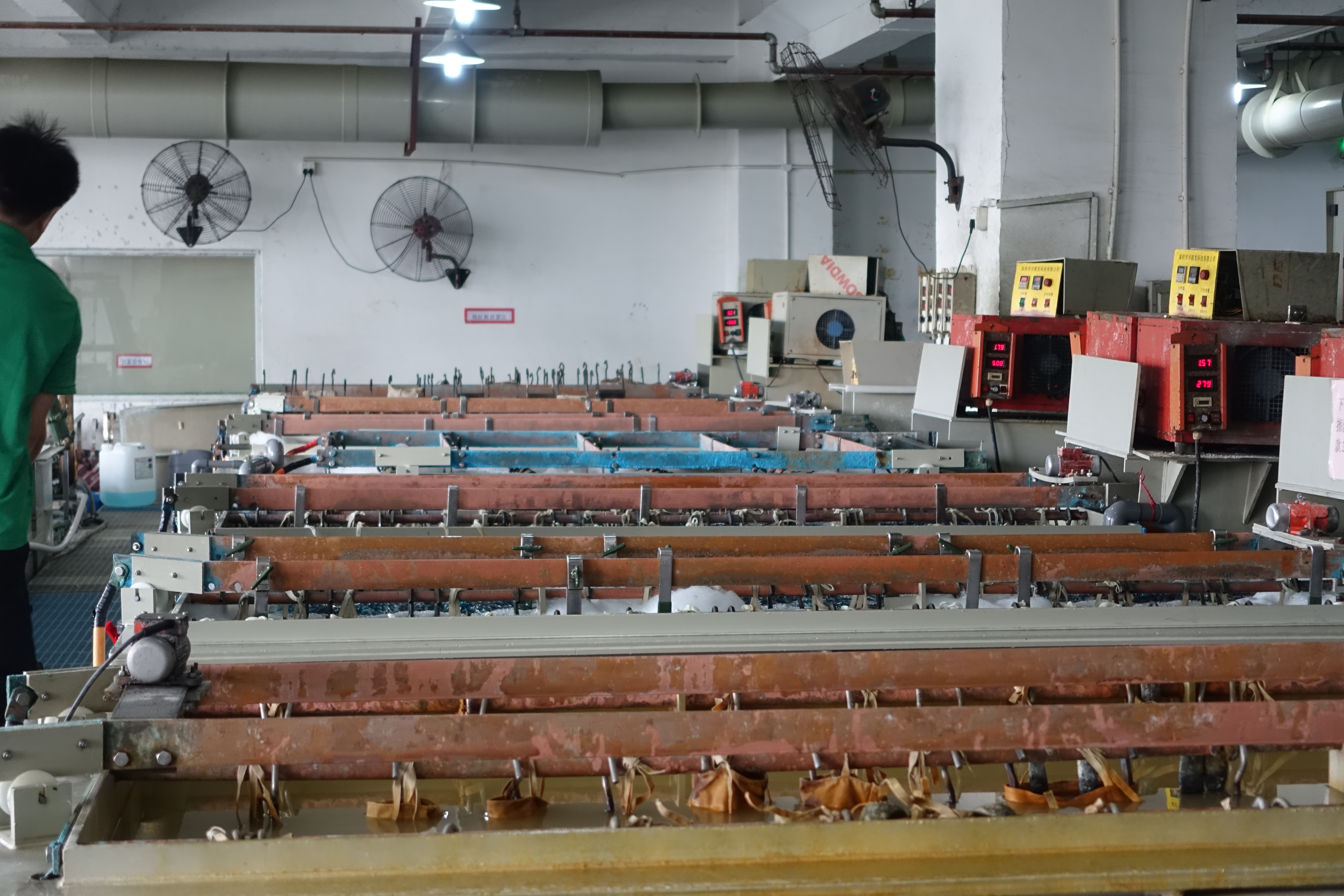
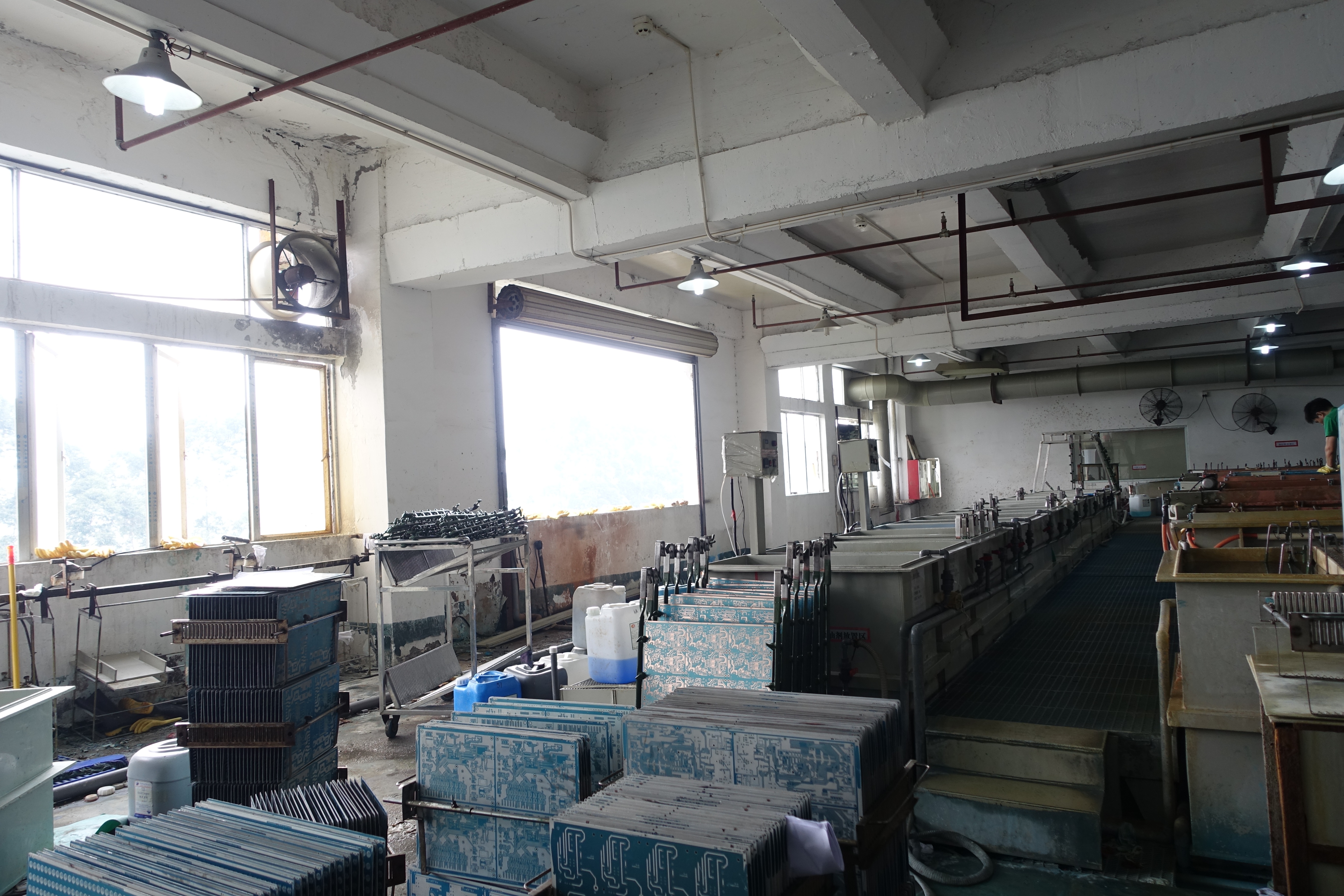
![DSC05887](https://i0.wp.com/dankc.com/wp-content/uploads/2016/08/DSC05887.jpg?resize=628%2C419&ssl=1)
Electroplating bath
![DSC05891](https://i0.wp.com/dankc.com/wp-content/uploads/2016/08/DSC05891.jpg?resize=628%2C419&ssl=1)
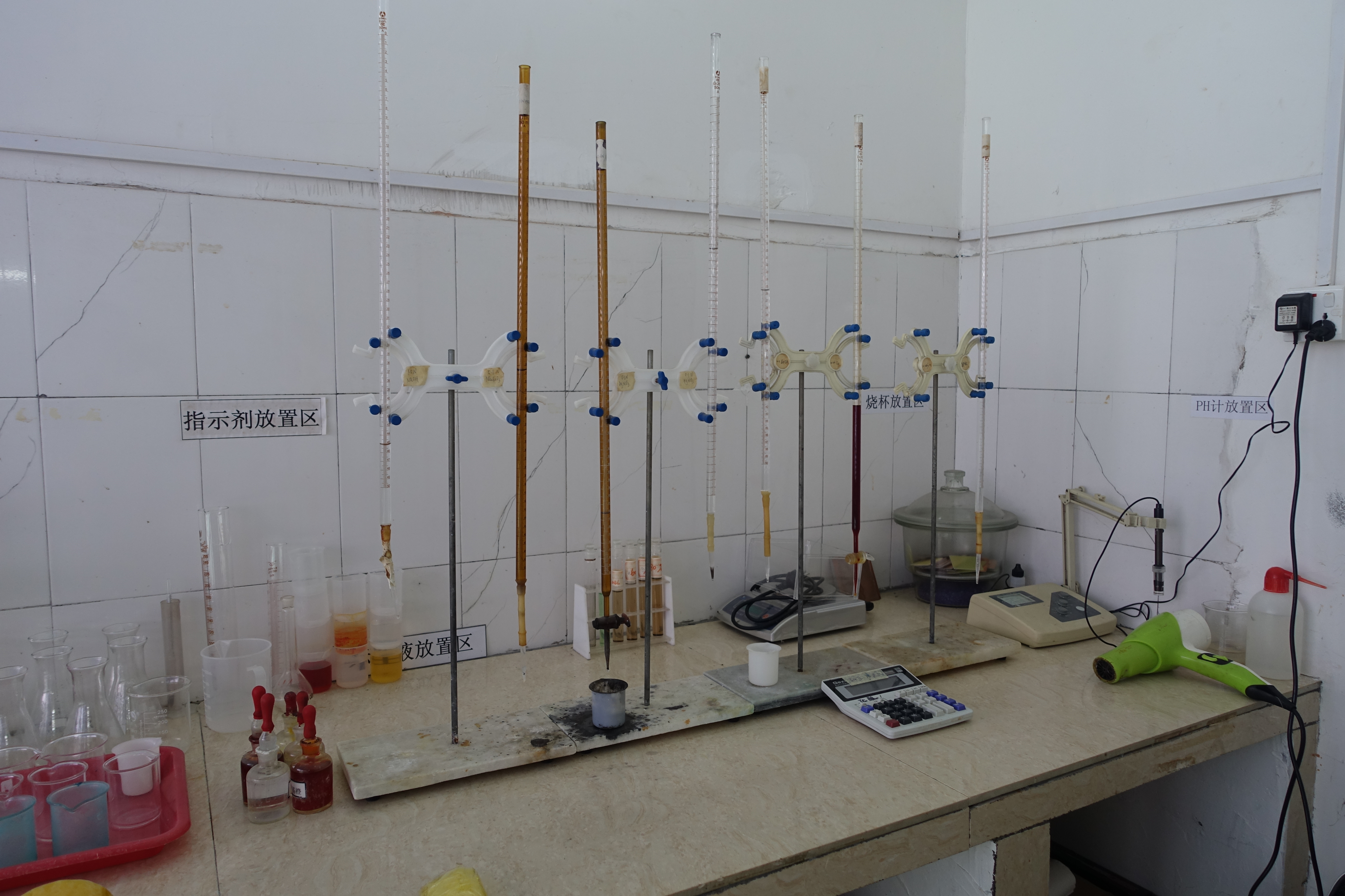
Here they figure out the solution for electroplating
![DSC05895](https://i0.wp.com/dankc.com/wp-content/uploads/2016/08/DSC05895.jpg?resize=628%2C419&ssl=1)